Silicon's Last Stand: The Materials Science Race to Outrun the Transistor's Physical Limits
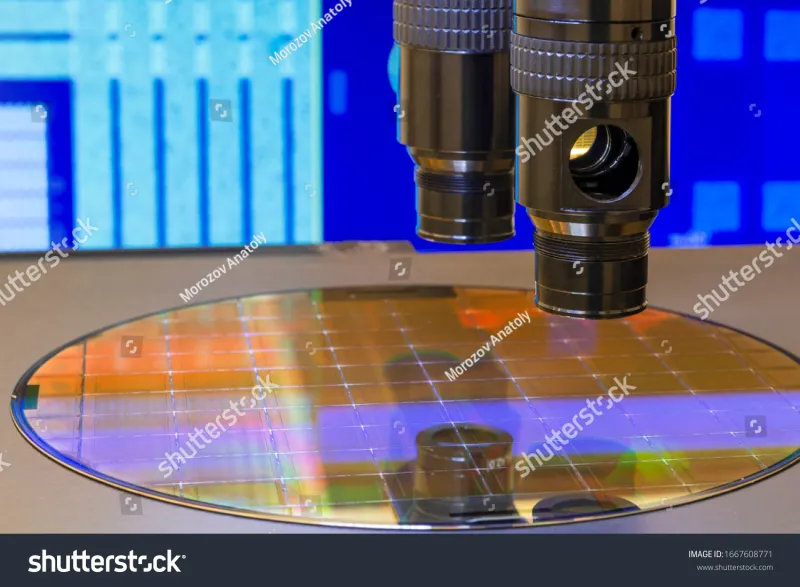
Photo: semiconductor chip nanoscale electron microscope silicon wafer laboratory, via www.shutterstock.com
For seven decades, the semiconductor industry has operated on a deceptively simple premise: make transistors smaller, and computing gets faster, cheaper, and more energy-efficient. That premise has held with remarkable fidelity. But as chipmakers approach the 1-nanometer scale—a dimension roughly equivalent to ten silicon atoms placed side by side—the premise is beginning to fracture under the weight of quantum mechanics.
The challenge is no longer purely one of engineering precision. It is, at its core, a confrontation with physics itself.
When Electrons Stop Following Orders
At dimensions below approximately 5 nanometers, a phenomenon known as quantum tunneling becomes increasingly disruptive to transistor behavior. Electrons, which in classical physics should be blocked by the thin insulating barrier between a transistor's gate and channel, instead probabilistically pass through it. They do not breach the barrier in any conventional sense—they simply appear on the other side, as quantum mechanics permits.
The consequence for chip designers is significant: transistors begin leaking current even when switched off. That leakage generates heat, wastes power, and introduces logic errors that compound at scale. In a chip containing tens of billions of transistors, even a fractional increase in per-unit leakage accumulates into a thermal management problem of considerable magnitude.
Intel, TSMC, Samsung, and IBM have each invested heavily in architectural solutions to mitigate this effect. Gate-all-around (GAA) transistors, which surround the channel with a gate on all four sides rather than three, improve electrostatic control and reduce leakage compared to the FinFET designs that dominated the previous generation. TSMC's 2-nanometer process, expected to enter volume production in 2025, relies on GAA nanosheet transistors. IBM demonstrated a functional 2-nanometer chip in 2021, claiming up to 45 percent performance improvement over its 7-nanometer predecessors.
But GAA is widely understood to be a refinement, not a reinvention. The underlying material—silicon—remains the same, and silicon's fundamental electronic properties impose ceilings that geometry alone cannot raise.
The Search for a Better Atom
The most consequential research currently underway in American semiconductor labs involves replacing silicon with materials that behave more favorably at extreme scales. Several candidates have moved from theoretical interest to active prototyping.
Gallium oxide has attracted attention for its exceptionally wide bandgap, which makes it highly resistant to electrical breakdown and well-suited for power electronics. Researchers at institutions including the University of Buffalo and the Air Force Research Laboratory have demonstrated gallium oxide transistors capable of handling voltages that would destroy silicon equivalents. Its limitation is electron mobility—charge carriers move more slowly through gallium oxide than through silicon, constraining switching speed.
Carbon nanotubes offer a different proposition. Semiconducting single-walled carbon nanotubes exhibit electron mobility several times higher than silicon, and their one-dimensional structure naturally limits short-channel effects that plague conventional transistors at small scales. IBM's research division has published work demonstrating carbon nanotube transistors operating below 10 nanometers with performance characteristics that silicon cannot match at equivalent dimensions. The manufacturing challenge—producing sufficiently pure, uniformly aligned nanotube arrays at wafer scale—has slowed commercialization, though progress has been measurable.
Transition metal dichalcogenides (TMDs), including molybdenum disulfide and tungsten diselenide, are two-dimensional materials that can be reduced to a single atomic layer without losing their semiconducting properties. Unlike silicon, which degrades rapidly as its thickness approaches atomic dimensions, TMDs remain electronically stable. MIT and Stanford have both published research demonstrating functional transistors built from monolayer TMDs, and several US-based startups are now attempting to scale these materials toward manufacturable processes.
Architecture as the New Frontier
Beyond material substitution, a parallel strategy involves rethinking chip architecture at the system level. Three-dimensional integration—stacking multiple layers of logic and memory vertically and connecting them with dense arrays of microscale interconnects—effectively sidesteps the per-layer scaling problem by adding a spatial dimension to performance gains.
AMD's 3D V-Cache technology, which stacks additional cache memory directly atop processor dies, demonstrated that vertical integration can deliver meaningful performance improvements without requiring further lithographic shrinkage. Intel's Foveros packaging technology pursues a similar logic, enabling heterogeneous chiplet designs where different functional blocks, potentially manufactured at different nodes or from different materials, are integrated into a single package.
This chiplet approach has implications beyond performance. It allows designers to optimize each functional block independently—using the most advanced silicon process for compute-intensive logic while employing more mature, cost-effective nodes for analog or I/O components. The result is a modular architecture that partially decouples overall system capability from any single material or process node.
Quantum and Neuromorphic Trajectories
For a subset of applications, the most consequential response to silicon's limits may be abandoning the classical computing paradigm altogether. Quantum computing, which encodes information in qubits that exploit superposition and entanglement, operates on fundamentally different physical principles. Companies including IBM, Google, and IonQ are advancing quantum processors that, for specific problem classes, may eventually outperform any classical silicon alternative regardless of transistor density.
Neuromorphic computing represents a third trajectory. Chips designed to mimic the architecture of biological neural networks—processing information through spiking signals rather than binary clock cycles—can perform certain inference and pattern-recognition tasks with orders of magnitude less power than conventional processors. Intel's Loihi 2 chip and IBM's NorthPole processor are among the more mature commercial examples of this design philosophy.
Neither quantum nor neuromorphic computing is positioned to replace general-purpose silicon chips in the near term. But both represent credible long-term alternatives for workloads where silicon's scaling limitations become prohibitive.
The Economic Stakes of Getting This Right
The United States has significant national interest in the outcome of these research trajectories. The CHIPS and Science Act, signed into law in 2022, allocated approximately $52 billion toward domestic semiconductor manufacturing and research, with a substantial portion directed toward advanced packaging, materials research, and workforce development. The underlying rationale was explicit: leadership in semiconductor technology is inseparable from leadership in defense capability, artificial intelligence, and economic competitiveness.
Labs at DARPA, the National Science Foundation, and the Department of Energy are all funding research programs aimed at post-silicon computing substrates. The timeline for any of these alternatives reaching high-volume manufacturing remains uncertain, but the institutional commitment to solving the problem is not.
The transistor has survived every predicted death since Jack Kilby built the first integrated circuit at Texas Instruments in 1958. Whether that survival continues through the 1-nanometer threshold—or whether it ends there and something more capable takes its place—will be determined in the research facilities operating today. The physics are unforgiving. The ingenuity being applied to them is formidable.